Recently I had the need to install an option ROM into my newly repaired 286, so that it could boot from IDE devices. That journey wasn't quite as straightforward as I had expected, so I thought I would write down what I'd done in case anyone else has a similar issue one day.
The fine folks at the XTIDE project have produced code suitable for use as an option ROM, which means if you can get it to appear in the PC's address space between C0000 and F0000 then the system BIOS will run the code automatically during the boot process, thus allowing booting from any installed IDE controller cards.
The easy option would have been to purchase a Lo-tech ISA ROM board, which allows a brand new EEPROM-compatible flash chip to appear in the correct address space. However I have many ISA network cards with boot ROM sockets, and since I intend to have a network card in each of these PCs anyway, I could save an expansion slot by putting the XTIDE ROM on the network card instead.
The complication arises as soon as you realise that almost all boot ROM sockets are 28-pin, and almost all 28-pin chips are older style EEPROMs, which require 12V to program and in many cases UV to erase. Since I don't have the hardware for this, my idea of reusing an old 28-pin chip was a dead end. I had previously used a PCI Realtek 8139 to dump 28-pin ROM chips, and this explains why it didn't seem to be capable of writing to them as well.
It turns out that most EEPROMs are standard 32-pin devices, and you can still buy them new for a few dollars each. Looking closely at the datasheets, I thought it might be possible to fit a 32-pin EEPROM into a 28-pin socket, if a few additional connections were made. With this plan in mind, I went ahead and purchased a handful of the same SST39SF020A chips used by the Lo-tech board, as well as some 32-pin EEPROM sockets to base my adapter on.
As it turns out, the adapter is very simple. You only need to connect all the overhanging pins together, and tie them to VCC (pin 28 on the 28-pin version.) One of these pins is the write enable line, so this means it is not possible to flash the chip in a 28-pin socket. It also means if you modify the chip directly, it will no longer be possible to reflash it. By modifying a 32-pin IC socket instead, the chip can be removed and reflashed as needed in a native 32-pin programmer.
This is the pinout of the two chip types:


From here you can see that if we plugged the 32-pin chip into the 28-pin socket, with pins 1-2 and 31-32 overhanging the socket, all the data lines and most of the address lines match up. However VCC would arrive on pin 30 and the real VCC pin would be without power. To build an adapter we will need to at least connect power to the real VCC. Pin 31 also enables write mode when pulled low, so we can tie that to VCC as well to ensure the chip is always in read-mode.
Since pin 30 (where VCC is coming in from the 28-pin socket) is used for A17, and A17 is only needed to access storage capacity larger than 128kB, we can leave that connected to VCC for simplicity. The drawback of doing this is that we will "limit" our storage capacity to 128kB, however this is not really a limit, because the 28-pin socket does not have an A17 line so it can only access a maximum of 128kB anyway.
The A16 and NC (pin 1, used for A18 in 512kB chips) should also be tied to something, so we will use VCC as well since it is close by. If we didn't do this and left the pins unconnected, they will "float" and could change value unexpectedly. This would effectively make the contents of the ROM vanish momentarily, causing the PC to lock up if it happened to be running code from the chip at the time.

Connecting all these pins together looks like this: (connections shown in red)

As mentioned previously, making these connections directly to a chip will prevent it from being reflashed, so for maximum flexibility a 32-pin PDIP socket should be modified so the flash chip can be removed as needed. The 32-pin PDIP socket fits nicely into a 28-pin socket, which means the only parts required to construct this adapter are the 32-pin socket itself and some very short lengths of wire.
After making the necessary connections, the adapter should look like this:

This picture is of course looking from the bottom up, so the connections are mirrored compared to the top-down view shown in the earlier diagrams. This adapter mounts nicely in a 28-pin EEPROM socket:

It also doesn't stick out much farther than normal, so it just fits in the available slot space without interfering with the neighbouring slot.
In my case, after having flashed the XTIDE BIOS, the 286 recognised the option ROM on the first attempt and happily ran it during the boot process!
Flashing the chip
To actually flash the chip, I used the fine flashrom tool.
Unfortunately my first attempt was to use a 3Com 3C905 Ethernet card as it was the only one I had with a 32-pin EEPROM socket, however I discovered that this card lacks the A17 address line, restricting its ability to flashing chips that are 128kB or smaller. Since I had a 256kB chip, and the 28-pin adapter requires the content placed in the upper-most address, I couldn't put the XTIDE code in the upper 128kB if the 3Com card could only flash the lower 128kB of the chip!
I then noticed the motherboard I was using - a Gigabyte GA-6BXC - had a 32-pin BIOS chip. Flashrom supports the Intel PIIX4 chipset used by this motherboard, so I could hot-flash the chip using the motherboard's BIOS socket.
I had never hot-flashed a machine before, but the process was very simple. Once Linux had started booting, the motherboard BIOS chip was removed, and the target EEPROM carefully placed in the socket. I didn't push it all the way in, just enough to make contact. Flashrom detected the chip, wrote the content and verified it again without complaint, so I could be sure the content was flashed successfully and the chip was easy to remove again. Since I had to buy the flash chips in a pack of 5, I used the hot-flash process to flash all five chips. One of them was bad - flashrom couldn't recognise it and the chip got very hot very quickly, but the other four were fine (and yes I tried three times and the chip was definitely in the right way.)
Since the XTIDE BIOS is only 8kB (or 12kB for the "large" version), it needs to be padded up to the size of the flash chip - 256kB in my case. I used a simple shell script for this:
$ (for ((I=12288; $I<16384; I=$[$I+1])); do echo -en "\xFF"; done) > pad.bin
$ cat ide_atl.bin pad.bin > xtide-16k.bin
$ cat xtide-16k.bin xtide-16k.bin xtide-16k.bin xtide-16k.bin > xtide-64k.bin
$ cat xtide-64k.bin xtide-64k.bin xtide-64k.bin xtide-64k.bin > xtide-256k.bin
This creates a 256kB file, with the complete XTIDE ROM at every 16kB mark. This means we only need to tell the Ethernet card the boot ROM is 16kB in size, and it won't need to take up a huge amount of memory which could otherwise be used for UMBs. Technically we could have done the calculations to get the XTIDE code to sit at exactly the 128kB mark, but since the rest of the chip is going to be ignored, it doesn't matter if we have duplicate data in there anyway.
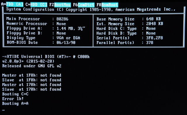
I flashed this 256kB file to the chip and placed it in the network card's boot ROM socket, and to my surprise everything worked the first time. You can see in the output of Norton Utilities' SI that there is an option ROM at address C800 (along with the video BIOS at C000 and the system BIOS at F000):
Part of the reason for the early success was because I had already found the configuration program for my network card and enabled the boot ROM socket, which was disabled by default. Finding the program to do this was a bit of a challenge, and I'm considering starting a wiki-like card database to assist with this issue.
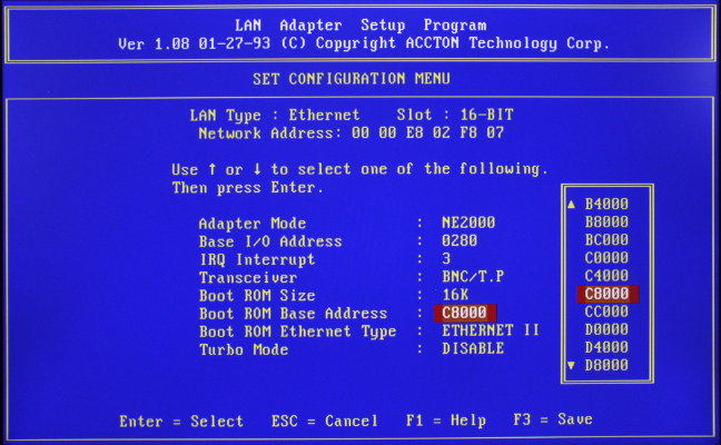
In my case (and to help anyone from Google), the card had an EN50903 chipset, with "A.T.C." on it (which stands for Accton Technology Corporation.) It turns out the EN50903 is used on a few cards, but mine was an Accton EN1640. Googling for en1640.zip got me the DOS drivers with the setup program, allowing me to set the port address, IRQ, and enable the boot ROM. Since my VGA BIOS stopped at segment C800, I put the boot ROM there and set it to 16kB. (Side note: it turns out the EN50903 is happy running in 8-bit mode, so this solution should also work for an XT, even though the card has a 16-bit ISA connector.)
Now I can start using IDE devices with my 286!
"(for ((I=12288; $I<16384; I=$[$I+1])); echo -en "\xFF"; done) > pad.bin" is not working
ReplyDelete"Syntax error: >>echo<< unexpected"
Whoops, missed the word "do" in the middle there - updated the post, thanks!
DeleteThanks for this guide!
ReplyDeleteI used a 3Com 3C905b-XT Ethernet card to flash a SST39SF010A (128kb) with flashrom. The rom is placed on a ISA 3com Etherlink III Card (3c50b-Combo) card. Works perfekt in my old 486. :)
I have some hints:
- Flashrom supports only 3Com "3C905b" Ethernet cards. The "b" is importend, "3C905" cards did not work.
- use the latest XTIDE binary from https://www.lo-tech.co.uk/wiki/XTIDE_Universal_BIOS . The official "XTIDE 2.0.0 Beta 3" is very old and had some issues.
I couldn't get this to work with the linux commands and the 12KB file in OpenSuse. However, I did get it to work this way:
ReplyDelete-Got the 8KB ide_at.bin EXTIDE file and used DOS TYPE to basically do what you did in Linux, buffer it with itself until it was the file size needed for the ROM.
-TYPE ide_at.bin ide_at2.bin >> ide_at3.tmp (now a 16KB file...)
-COPY ide_at3.tmp ide_at4.tmp (make a duplicate file, both 16KB...)
-TYPE ide_at3.tmp ide_at4.tmp >> ide_at5.tmp (now a 32KB file..)
...son on until I got a 256KB file from the 8KB XTIDE ide_at.bin file.
I used the exact card Chris had (3COM 3C905B-TX...not XT...) with an SST39SF020A 256K with the FLASHROM program. My exact DOS commands with the file i created with the above method in dos, now renamed xtide256.bin
flashrom -r xtide256.bin -p nic3com -f
It flashed the chip just fine, i rebooted. I then bridged the ROM with the above schematic (i didn't use an adapter...), and put it into a Kingston KNE-2031+ ISA ethernet card that only had the 28 pin socket. I booted it in my 386 system and success! Found an attached 4GB CF card I had with a CF-IDE adapter on a generic 16bit isa IDE card. I tried in my 486 system too, and found it just fine.
However, when i rebooted right after I flashed the chip in the 3COm 3C305b-TX card, it booted the rom but froze the system. It was a Pentium-3 system with an ISA slot, so XTIDE bios not be the most compatible with that system.
Anyways, thanks for the blog. That schematic helped me greatly.
Thanks for the DOS instructions! You might also want to consider using COPY /B instead of TYPE, as I believe TYPE will stop if it encounters an EOF byte, while COPY will process the whole file.
DeleteNot sure why it didn't work in a Pentium 3 - perhaps the card's ROM window was too large or too small?
I'm going to test that out tonight. I didn't have much time to look at how much memory was taken up. It should only be the 16K as specified by the setup program for the Kingston KNE-2031+...btw, it was HORRIFIC to find the program that actually worked with the KNE-2031+. Its called AUTOSET.EXE for anyone looking for it. Every other Kingston program couldn't find the adapter.
DeleteBTW, I didn't know you posted this to VOGONS back in December! I just happened upon that post doing a google search. Nice to see a fellow Vogon.
Good to know about COPY /B. I knew it was an option, but thought I'd try the TYPE instead.
Yes some of those old network utilities are very hard to find. This is one of the reasons why I started the Vogons Device Library, to hopefully make this sort of thing a bit easier. If you have already found the utility for your card, I strongly encourage you to add it to the library! Just copy an entry like this one and update it. Feel free to post on Vogons or e-mail me directly with the details if you need the config utility added to Vogonsdrivers.
Delete